By Dr. Kathleen Vaeth, Director of OLED UX
Whenever I enter a new field or join a new organization, the first thing that often strikes me is the number of acronyms and related jargon. The time-saving alphabet soup of shorthand words that so easily trip off the tongue can sometimes be one of the hardest parts of coming up to speed. In some cases, an acronym can stand for very different things in different settings, leading to puzzled looks, quick internet searches, and often, a good laugh.
In lighting, a common acronym-related inquiry is what the difference is between light emitting diodes (LEDs) and organic light emitting diodes (OLEDs). More than just shorthand, awareness of the fundamentals of these technologies helps in understanding what each has to offer for lighting our products and our world.
Inorganic and Organic LED Technologies
A diode is an electrical structure that allows current to flow easily in one direction, but not in the opposite – an electrical switch. It consists of two materials placed in contact with each other, with one better transporting negative charges, and another better at transporting positive charges. In modern electronics, these materials are solids, and incorporated as layers that are a few to tens of nanometers thick. Additional layers are often placed in between the two materials to further tailor the diode operation.
In LEDs and OLEDs, some of the additional layers in the device can convert electricity into visible light, through a process known as electroluminescence (EL). This happens when current injected into the material creates an excited state, which then relaxes to produce a photon. The specific emission wavelength depends on the properties of the material, and the amount of light generated is generally proportional to the amount of injected current. LED and OLED performance depends on both the EL efficiency of the emitter material and how well charge movement and excited state formation are controlled spatially within the device. Since light emission comes from solid materials instead of electrically excited gasses in evacuated cavities, illumination based on LEDs and OLEDs is typically referred to as solid state lighting (SSL).
Although the discussion above applies to all types of light emitting diodes, both inorganic and organic, in the microelectronics, lighting and display world, the term ‘LED’ usually refers to a device made entirely from inorganic materials. This is because inorganic LEDs have been around longer, with the first practical devices reported in the early 1960s, compared to the late 1980s for OLEDs. The materials used in inorganic LEDs are compounds based on combinations of gallium (Ga), aluminum (Al), indium (In), nitrogen (N), phosphorous (Ph), and arsenic (As) – the so-called ‘III-V’ materials due to their group placement in the periodic table. The layers are crystalline in form, grown atom-by-atom under vacuum from gaseous metalorganic precursors in a process known as chemical vapor deposition (CVD). The regular arrangement of the atoms creates a delocalized electronic structure which defines the optoelectronic properties of the material. The emission color depends on the elements present and their ratios, with InGaN systems producing shorter, blue/green EL, and GaP and AlGaAs systems exhibiting yellow and red EL.
The emission efficiency depends in part on how perfectly the crystal is grown during deposition, as defects or kinks allow the excited state to relax without producing light, which reduces the EL efficiency. In fact, to produce low crystal defect III-V layers, the material must be grown on a substrate with a crystal spacing similar to the desired compound, typically sapphire wafers seeded with a thin layer of GaN for LEDs used in general lighting applications. There is quite a bit of variation in the performance of inorganic LEDs due to these defects, and testing and binning of the devices is an important part of the manufacturing quality control process.
With OLEDs, the diode materials are molecules that contain mostly carbon, nitrogen, and hydrogen, linked together through chemical bonds. These connections are a mixture of single and double bonds, which create a delocalized electronic structure on the molecules that defines their optoelectronic properties. OLED layers are formed by subliming the molecules under low vacuum in a process known as thermal evaporation. Unlike III-V compounds, OLED molecules are not required to be well-ordered for efficient light emission, instead depositing as an amorphous layer. This does make the layer less conductive compared to inorganic LED compounds, and requires use of more water-sensitive metals for the negative charge injection electrode. Emission color is controlled at the molecular level instead of the atomic level with co-evaporated blends of an organic host and dopant optimized for efficient scavenging of the excited state. The evaporation process used to create the OLED emission layer is a well-controlled and repeatable process. Since the materials are amorphous, no lattice matching is required, which widens the types of substrates that can be used. The amorphous layers also allow a degree of mechanical flexibility, and OLEDs have been fabricated on flexible substrates.
The Big Difference – Layer Order
Discussions of inorganic LEDs and OLEDs often emphasize the difference in atomic composition of the material, organic vs. inorganic, and it is important. The inorganic compounds are more stable to water and oxygen during device operation, making encapsulation requirements for OLEDs comparatively more stringent. Interestingly, these requirements are driven primarily by the need to protect against corrosion of the metal used for the OLED electrode, and not the organic materials themselves. This is why despite the ability to be coated on many substrates, OLEDs are mainly fabricated on those with ultra-high resistance to water and oxygen transmission, such as glass and barrier-coated plastics. OLED encapsulation was a big challenge in the early days of the technology, but methodologies and materials such as thin barrier coatings and metal foils have been developed over the years to address the issue, such that this is no longer a factor for device lifetimes.
While the elemental composition of the material used with the technologies is important, I believe a more critical issue to understand is the difference in material layer order between inorganic LEDs and OLEDs—crystalline vs. amorphous—as it has significant consequences for how the diodes can be built and subsequently integrated into SSL products. This is because the required material layer order for efficient EL determines how big the emission area from the device can be.
With inorganic materials, the crystalline area that can be grown with low enough defect density for efficient EL using the CVD process is extremely small – typically on the order of a few square millimeters. This limits the size of state-of-the-art inorganic LEDs to that range, and as a result, the light output is a point source that is very directional in nature. The amorphous organic layers used in OLEDs do not have this constraint and can be coated over thousands of square millimeters, limited more by the cleanliness of the substrate and manufacturing process. The result is a huge diode with a diffuse emission.
Impact on Lighting Applications
For applications such as lighting, where a large area of illumination is often required, this emission area difference drives very different approaches for product design and integration, and in the end, different form factors and lighting experiences. To get a larger emission area with inorganic LEDs, several of the small devices must be assembled into an array and driven as point sources of illumination. The light is then diffused with a separate optical component to smooth the output over the desired illumination area for the fixture. This process does have optical losses associated with it, which can lower the overall efficacy of the fixture compared to that of the individual LEDs. However, the individual inorganic LEDs are highly efficient, and SSL fixtures constructed with them can still achieve high overall efficacy.
Depending on the design, illumination is generated in only a small fraction of the entire fixture area with inorganic LEDs, which has several consequences. First, the area around the LED gets hot, requiring additional components in the assembly for thermal management such as heat sink blocks. The additional components add bulk, weight and thickness to the fixture, as well as complexity, the latter of which is important in fixture reliability and ease of handling at end-of-life. Second, even with optical diffusion, the illumination can still be fairly directional and high in glare, contrast, and shadows, which can cause eye discomfort and strain.
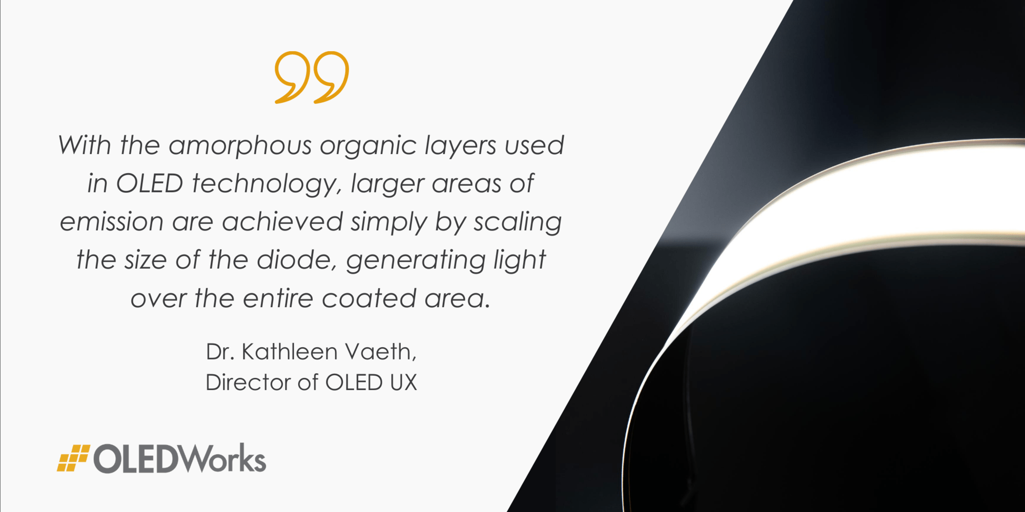
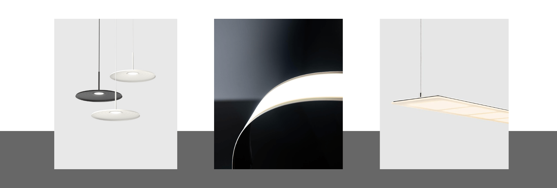
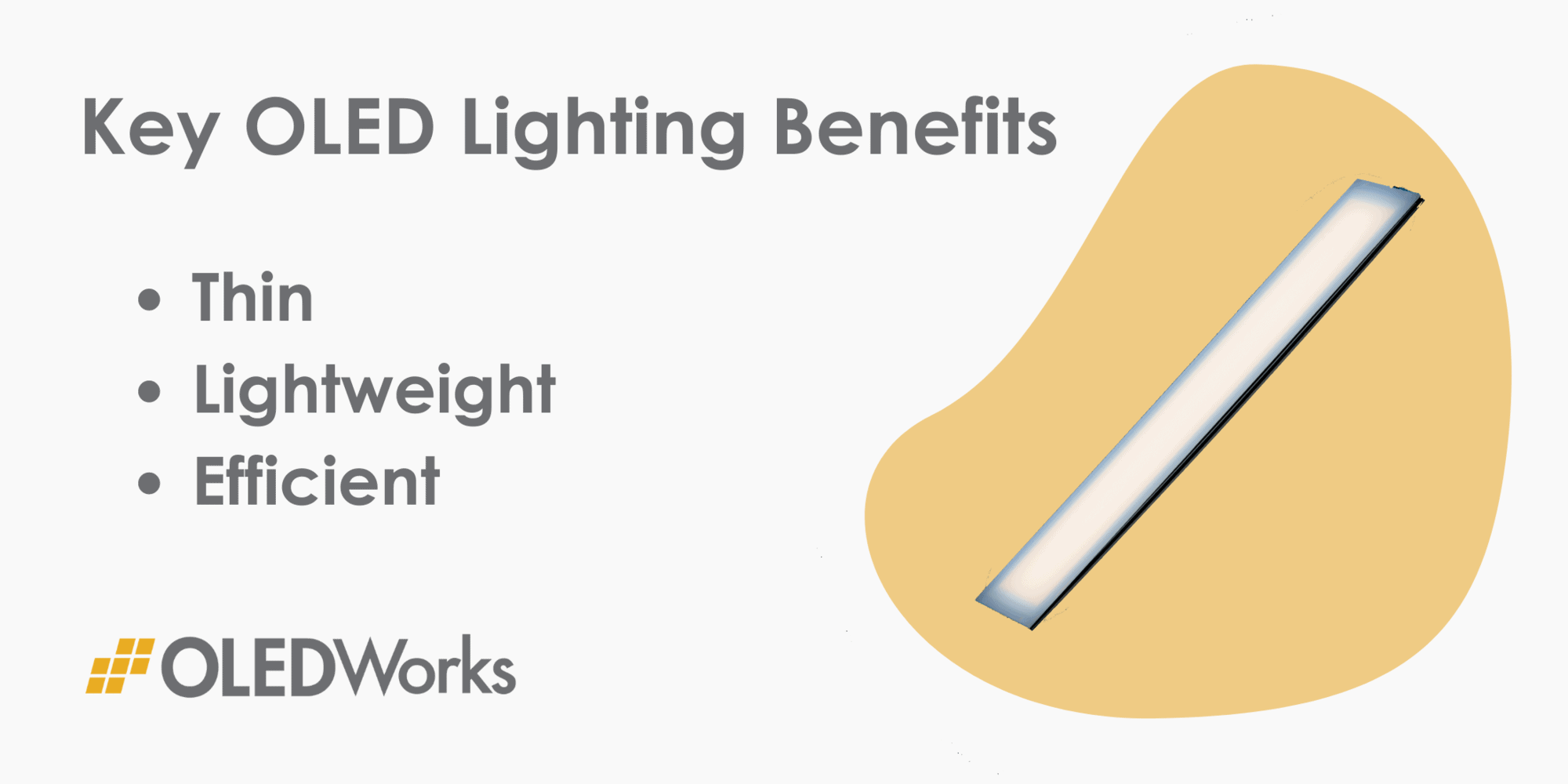
With the amorphous organic layers used in OLED technology, larger areas of emission are achieved simply by scaling the size of the diode, generating light over the entire coated area. The illumination is naturally diffuse, free from glare and low in contrast, even on curved or flexible substrates. OLED lighting panels often incorporate additional light extraction layers internal or external to the device, which significantly reduce waveguiding out the edges of the substrate and improving the overall panel efficacy. These materials are similar in thickness to the organic layers and applied during the panel manufacturing process.
Since emission comes from the entire surface of the panel, there are no point sources or local hotspots. Therefore, there is no need to scatter the light, keeping panel efficacy high, or to incorporate additional components such as diffusers and heat sinks. This makes OLED lighting panels very thin and lightweight, with efficacies rivaling those of inorganic LED fixtures. The glare-free illumination has been shown to reduce eye strain, and this, combined with the uniform and diffuse illumination, gives flexibility for use in areas that may be more in the line of sight or close to the user. In fact, designs with OLED lighting panels can often be playful, highlighting the illumination source and using it for design inspiration.
To learn more about the differences between LED and OLED technologies, make sure to check out my next blog, which will cover the different approach each technology uses to create the broad spectrum emission required in general lighting, and what that means for overall fixture performance.